
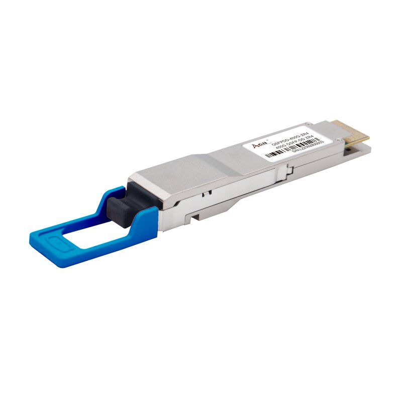
Optical SFP Module
400G QSFP-DD ZR4 Transceiver, DWDM C-band, 80KM
Share on
Features
Application
Standard
Absolute Maximum Ratings
| Parameter | Symbol | Min | Max | Unit |
| Storage Ambient Temperature | TSTG | -40 | 85 | ℃ |
| Operating Humidity | HO | 5 | 85 | % |
| Power Supply Voltage | Vcc | -0.3 | 3.6 | V |
| Signal Input Voltage | Vcc-0.3 | Vcc +0.3 | V |
Recommended Operating Conditions
| Parameter | Symbol | Min | Typical | Max | Unit |
| Operating Case Temperature | Tc | 0 | 70 | ℃ | |
| Power Supply Voltage | Vcc | 3.13 | 3.3 | 3.47 | V |
| Data Rate, each Lane(PAM4) | 53.125 | Gbps | |||
| Fiber Length 9/125μm core MMF | 80 | km |
Optical and Electrical Characteristics
| Optical Transmitter Characteristics | |||||
| Parameter | Min | Typical | Max | Unit | Notes |
| Transmitter Frequency Range | 191.3 | 193.7 | 196.1 | THz | C band 75GHz ITU-T grid. Frequency range over which the specifications hold unless noted otherwise. |
| Laser Frequency Stability | -1.8 | 1.8 | GHz | Frequency stability relative to ITU grid. | |
| Laser Frequency Accuracy | -1.8 | 1.8 | GHz | ||
| Laser Frequency Fine Tuning Range | -6.0 | 6.0 | GHz | ||
| Fine Tuning Resolution | 100 | MHz | |||
| Channel Tuning Speed | – | 60 | s | ||
| Laser LineWidth | 300 | kHz | |||
| Transmitter Output Power Range | -11.5 | dBm | |||
| Transmitter Laser Disable Time | 180 | ms | |||
| Output Power Stability | -0.5 | 0.5 | dB | Difference over temperature, time, wavelength and aging. | |
| Output Power Accuracy | -2 | 2 | dB | Difference between the set value and actual value over aging. | |
| Transmitter Turn-up Time from Cold Start | – | 100 | s | ||
| Transmitter OSNR (Inband) | 34 | – | dB/0.1nm | ||
| Transmitter Back Reflectance | – | -24 | dB | ||
| Transmitter Output Power with TX Disabled | – | -20 | dBm | ||
| Transmitter Polarization Dependent Power | – | 1.5 | dB | Power deference between X and Y polarization | |
| Optical Receiver Characteristics | |||||
| Parameter | Min | Typical | Max | Unit | Notes |
| Receiver Frequency Range | 191.3 | 193.7 | 196.1 | THz | |
| Input Power Range | -12 | 0 | dBm | Signal power of the channel at the OSNR Penalty < 0.5dB | |
| OSNR Sensitivity
| 26 | dB/0.1nm
| |||
| Receiver Sensitivity | -20 | dBm | Input power needed to achieve post FEC BER <1E-15 when OSNR Tolerance> 26dB/0.1nm | ||
| Los Assert
| -20 | -18 | -16 | dBm
| |
| Los Hysteresis
| 1.0 | 2.5 | dB
| ||
| CD Tolerance
| 2400 | ps/nm
| Tolerance to Chromatic Dispersion.
| ||
| PMD Tolerance | 10 | ps | Tolerance to PMD with < 0.5 dB penalty to OSNR sensitivity. | ||
| Peak PDL Tolerance | 3.5 | dB | Tolerance to peak PDL with < 1.3 dB penalty to OSNR sensitivity when change in SOP is < =1 rad/ms. | ||
| Tolerance to Change in SOP | 50 | rad/ms | |||
| Input Power Transient Tolerance | -2 | 2 | dB | Tolerance to change in input power with < 0.5 dB penalty to OSNR sensitivity. | |
| Input Power Reading Accuracy | -2 | 2 | dB | ||
| Optical Return Loss | -20 | dB | Optical reflectance at Rx connector input. | ||
| Receiver Turn-up Time from Cold Start | – | 100 | s | From module reset, with valid optical input signal present. | |
Ordering information
| Part. No | Specifications | ||||||
| Pack | Rate (Gbps) | Tx (nm) | Sen (dBm) | Temp (℃) | Reach (km) | DDM | |
| QSFPDD-400G-ZR4 | QSFP-DD | 400G | DWDM | <-20 | 0~70 | 80 | Y |
WhatsApp us
We will contact you within 48 hours

Note: Your email information will be kept strictly confidential.

Automated page speed optimizations for fast site performance
